Video 1: Mechanical is NOT Cooler than Electrical!
In this first video, we turned the voltage up to 10 volts which automatically triggered the relay. We were trying to figure out a way to drop something onto the dominoes and trigger the domino effect. We had everything set up, except how we would trigger the dominoes...
Video 2: Our Rube Goldberg Circuit
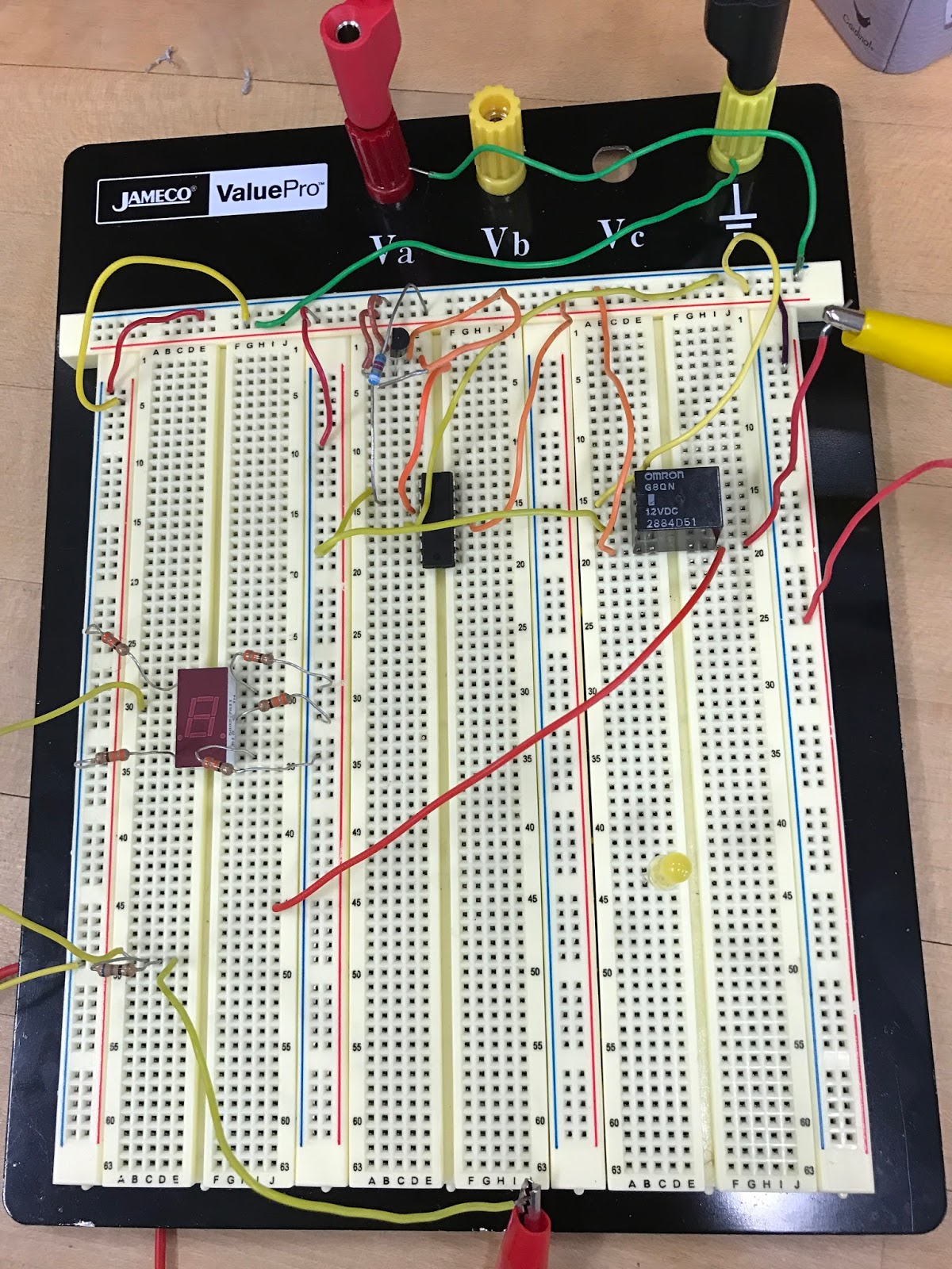
This is an up close video of the circuit we made. We have a temperature sensor that triggers the relay, which drops the brick onto the dominoes, which then triggers the pressure sensor and lights up our group number.
Video 3: Our First Problem with the Circuit
This was the first problem with the circuit that we encountered. When the motor started spinning it actually brought the brick into the motor and stead of away and dropping it onto the bricks. We realized that we had to just slightly hang the brick off of the motor so it spun out and dropped when the relay triggered it.
Video 4: It works!
Everything had finally started working on this try. We had carefully hung the brick onto the motor, and the dominoes had all fallen. The only thing we should have done differently was make the temperature sensor trigger the relay with the warmth of our fingers instead of the heat gun.
1. Force sensing resistor gives a resistance value with respect to the force that is applied on it. Try
different loads (Pinching, squeezing with objects, etc.) and write down the resistance values.
(EXPLAIN with TABLE)
Note: The harder you push down on the force sensing resistor, the less the resistance will be.
Force
Resistance (kΩ)
No Force
0
Light Touch
20.97
Medium Touch
8.72
Hard Touch
0.76
Pinch
0.26
the force sensing resistor gives only a measurement of 0L, or overload, when there is no force applied to it. As we apply more force to the sensor, the resistance value goes down. This means if we apply a set voltage to the sensor, more current will be able to flow through it as we apply a greater force.
2. 7 Segment display:
a. Check the manual of 7 segment display. Pdf document’s page 5 (or in the document page 4)
circuit B is the one we have. Connect pin 3 or pin 14 to 5 V. Connect a 330 Ω resistor to pin
1. Other end of the resistor goes to ground. Which line lit up? Using package dimensions and
function for B (page 4 in pdf), explain the operation of the 7 segment display by lighting up
different segments. (EXPLAIN with VIDEO).
Applying voltage to specific pins on the seven segment display, we can get different segments to light up. This will enable us to display numbers 0-9 later in the lab.
b. Using resistors for each segment, make the display show 0 and 5. (EXPLAIN with PHOTOs)
Depending on where the resistors are located will determine what number is shown on the counter.
3. Display driver
(7447). This integrated circuit (IC) is designed to drive 7 segment display through
resistors. Check the data sheet. A, B, C, and D are binary inputs. Pins 9 through 15 are outputs that
go to the display. Pin 8 is ground and pin 16 is 5 V.
a. By connecting inputs either 0 V or 5 V, check the output voltages of the driver. Explain how
the inputs and outputs are related. Provide two different input combinations. (EXPLAIN
with PHOTOs and TRUTH TABLE)
Number
A
B
C
D
0
0
0
0
0
8
1
0
0
0
The four inputs create a 4-bit binary number--with D as the most significant digit and A as the least significant digit--that corresponds to the number displayed. Each combination of inputs, with "0" representing 0 V applied to that pin and "1" representing 5 V applied to the pin, generates a combination of seven outputs, activating up to seven of the pins 9-15 on the display driver. Each of these output pins corresponds to one of the pins.on the Seven Segment Display and will allow us to display the number 0-9 when connected correctly
pictures above is by using #0
pictures above by using #8
b. Connect the display driver to the 7 segment display. 330 Ω resistors need to be used
between the display driver outputs and the display (a total of 7 resistors). Verify your
question 3a outputs with those input combinations. (EXPLAIN with VIDEO)
We are able to change the output number based on where the resistors are connected. You see here that connecting a single resistor to a different output changes the number from 0 to 8.
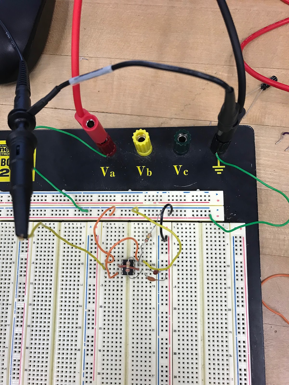
4. 555 Timer:
a. Construct the circuit in Fig. 14 of the 555 timer data sheet. VCC = 5V. No RL (no connection to
pin 3). RA = 150 kΩ, RB = 300 kΩ, and C = 1 µF (smaller sized capacitor). 0.01 µF capacitor is
somewhat larger in size. Observe your output voltage at pin 3 by oscilloscope. (Breadboard
and Oscilloscope PHOTOs)
b. Does your frequency and duty cycle match with the theoretical value? Explain your work.
A duty cycle is the percentage of the period when this 555 timer's signal is active. From our oscilloscope measurement, it seems as if our timer's signal is active closer to 60% of the time, when there is a reading of 5V and inactive closer to our calculated value of 40%, when the oscilloscope measured 0V. However, if you look at the next question, you can see that when our timer's signal is inactive, that is, we have not put any pressure on the force sensor, then the oscilloscope reads 5V and only begins to cycle between 0 and 5 V once we put pressure on the force sensor.
c. Connect the force sensing resistor in series with RA. How can you make the circuit give an
output? Can the frequency of the output be modified with the force sensing resistor?
(Explain with VIDEO)
With the force sensing resistor attached to the 555 timer's circuit, we need to apply pressure to the sensor in order to see an output. We found that the frequency increased very slightly when we applied a lot of force compared to only a small amount of force.
5. Binary coded decimal (BCD) counter (74192). This circuit generates a 4-bit counter. With every clock
change, output increases; 0000, 0001, 0010, …, 0111, 1000, 1001. But after 1001 (which is decimal
9), it goes back to 0000. That way, in decimal, it counts from 0 to 9. Outputs of 74192 are labelled as
QA (Least significant bit), QB, QC, and QD (Most significant bit) in the data sheet (decimal counter,
74192). Use the following connections:
5 V: pins 4, 11, 16.
0 V (ground): pins 8, 14.
10 µF capacitor between 5 V and ground.
a. Connect your 555 timer output to pin 5 of 74192. Observe the input and each output on the
oscilloscope. (EXPLAIN with VIDEO and TRUTH TABLE)
1. You will use the OPAMP in “open-loop” configuration in this part, where input signals will be applied directly to the pins 2 and 3.
a. Apply 0 V to the inverting input. Sweep the non-inverting input (Vin) from -5 V to 5 V with 1 V steps. Take more steps around 0 V (both positive and negative). Create a table for Vin and Vout. Plot the data (Vout vs Vin). Discuss your results. What would be the ideal plot?
Vin(V)
Vout(V)
5
4.48
4
4.48
3
4.48
2
4.48
1
4.48
0
0
-1
-3.88
-2
-3.88
-3
-3.88
-4
-3.88
-5
-3.88
Table 1:The data (Vout vs Vin) NON-inverting
Graph1: (Vout vs Vin) NON-inverting
b. Apply 0 V to the non-inverting input. Sweep the inverting input (Vin) from -5 V to 5 V with 1 V steps. Take more steps around 0 V (both positive and negative). Create a table for Vin and Vout. Plot the data (Vout vs Vin). Discuss your results. What would be the ideal plot?
Vin(V)
Vout(V)
-5
4.48
-4
4.48
-3
4.48
-2
4.48
-1
4.48
0
0
1
-3.88
2
-3.88
3
-3.88
4
-3.88
5
-3.88
Table 2: The data (Vout vs Vin) inverting
Graph2: (Vout vs Vin) inverting
2. Create a non-inverting amplifier. (R2 = 2 kΩ, R1 = 1 kΩ). Sweep Vin from -5 V to 5 V with 1 V steps. Create a table for Vin and Vout. Plot the measured and calculated data together.
Vin(V)
Vout(v)
Measured
Vout(V)
Calculated
5
4.23
5
4
4.23
5
3
4.23
5
2
4.23
5
1.5
4.23
5
1
3.03
3
.5
1.35
1.2
.25
0.8
1
0
0
0
-.25
-0.8
-1
-.5
-1.61
-1.2
-1
-3.2
-3
-1.5
-3.77
-5
-2
-3.77
-5
-3
-3.77
-5
-4
-3.77
-5
-5
-3.77
-5
Table3:The data (Vout vs Vin) NON-inverting
Graph3: (Vout vs Vin) NON-inverting
3. Create an inverting amplifier. (Rf = 2 kΩ, Rin = 1 kΩ). Sweep Vin from -5 V to 5 V with 1 V steps. Create a table for Vin and Vout. Plot the measured and calculated data together.
Vin(V)
Vout(v)
Measured
Vout(V)
Calculated
5
-3.7
-5
4
-3.7
-5
3
-3.7
-5
2
-3.7
-4
1.5
-3.06
-2.5
1
-1.99
-2
.5
-0.99
-1.2
.25
-0.51
-0.6
0
0
0
-.25
0.5
0.5
-.5
0.98
1
-1
2.16
2
-1.5
3.01
3
-2
4.06
5
-3
4.16
5
-4
4.16
5
-5
4.16
5
Table4:The data (Vout vs Vin) inverting
Graph4: (Vout vs Vin) inverting
4. Explain how an OPAMP works. How come is the gain of the OPAMP in the open loop configuration too high but inverting/non-inverting amplifier configurations provide such a small gain?
An OpAmp takes an input signal and amplifies it, providing a larger output signal. If the input signal is applied to the non-inverting input, then the output will have the same sign as the input. If the input is applied to the inverting input, then the output will have the opposite sign of the input. An OpAmp requires a source voltage in order to work and the output voltage cannot exceed the value of the source voltage. The gain of the OpAmp is determined by a ratio of the resistors used in an inverting/non-inverting amplifier configuration. This gain is what determines the factor by which the input voltage is multiplied to generate the amplified output voltage. Because an open loop configuration does not use any resistors to limit the effect of the amplifier, the gain is very high and the minimum and maximum output voltages are reached very quickly.
schematic view is the bottom view!
1. Connect your DC power supply to pin 2 and ground pin 5. Set your power supply to 0V. Switch your multimeter to measure the resistance mode; use your multimeter to measure the resistance between pin 4 and pin 1. Do the same measurement between pin 3 and pin 1. Explain your findings (EXPLAIN).
4-1 - 1.2 ohms
3-1 is not reading anything
2. Now sweep your DC power supply from 0V to 8V and back to 0V. What do you observe at the multimeter (resistance measurements similar to #1)? Did you hear a clicking sound? How many times? What is the “threshold voltage values” that cause the “switching?” (EXPLAIN with a VIDEO).
The voltage clicks when you approach 6 V, and it clicks when you are going back down and are approaching about 2.5 V. It was like this for both pins. For pins 1-3, it starts off with a 0 Ohm measurement. Once it clicks after 6 volts, you can measure the resistance for pins 1-3, and it is the exact opposite for 1-4. For 1-4, you can measure the resistance only before it clicks, and after it comes back from the second click.
3. How does the relay work? Apply a separate DC voltage of 5 V to pin 1. Check the voltage value of pin 3 and pin 4 (each with respect to ground) while switching the relay (EXPLAIN with a VIDEO).
For pin 3, at 0 Volts we have around 100 mV. When approaching 6 volts, The voltage reading actually goes to a negative voltage and once clicks, it stays at 5 Volts. The same is when sweeping back down, when it clicks the 5 Volts turns into a negative mV value and when it hits 0 volts it hovers around 100 mV. For pin 4, it is the exact opposite. At 0 Volts on the sweep, the voltage reading is 5 Volts. When it clicks at 6 Volts, the voltage changes to a negative small mV value, and it stays that way until it clicks again on the sweep down and stays at 5 Volts.
LED + Relay
1. Connect positive end of the LED diode to the pin 3 of the relay and negative end to a 100 ohm resistor. Ground the other end of the resistor. Negative end of the diode will be the shorter wire.
2. Apply 3 V to pin 1
3. Turn LED on/off by switching the relay. Explain your results in the video. Draw the circuit schematic (VIDEO)
We have 3 Volts going to pin 1, and are sweeping the voltage at pin #2. Once pin #2 hits 6 volts, the relay is turned on and so is the LED light. Once the voltage is sweeping down to 2 Volts, the Relay clicks and and the light is turned off.
Operational Amplifier (data sheet under Bb/week 6)
1. Connect the power supplies to the op-amp (+10V and 0V). Show the operation of LM 124 operational amplifier in DC mode with a non-inverting amplifier configuration. Choose any opamp in the IC. Method: Use several R1 and R2 configurations and change your input voltage (voltages between 0 and 10V) and record your output voltage. (EXPLAIN with a TABLE)
R1=2kohms, R2=12kohms
Vin(V)
Vout(V)
0
0.5
1
7.89
2
9
3
9
4
9
5
9
6
9
7
9
8
9
9
9
10
9
R1=1kohms, R2=2kohms
Vin(V)
Vout(V)
0
0.23
1
.89
2
2.5
3
9.37
4
9.37
5
9.37
6
9.37
7
9.37
8
9.37
9
9.37
10
9.37
R1=12kohms, R2=1kohms
Vin(V)
Vout(V)
0
0.8
1
1.2
2
2.4
3
3.1
4
4.2
5
5.3
6
6.4
7
7.8
8
8.5
9
8.8
10
8.9
3. Design a system where LED light turns on when you heat up the temperature sensor. (CIRCUIT schematic and explanation in a VIDEO)